- 您现在的位置:买卖IC网 > Sheet目录1904 > ATF1502ASV-15JI44 (Atmel)IC CPLD EE HP 15NS 44-PLCC
6
1615J–PLD–01/06
ATF1502ASV
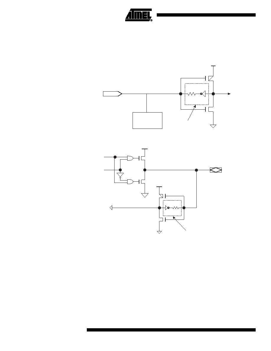
floating to intermediate voltage levels, which causes unnecessary power consumption and sys-
tem noise. The keeper circuits eliminate the need for external pull-up resistors and eliminate
their DC power consumption.
Figure 2-1.
Input Diagram
Figure 2-2.
I/O Diagram
3.
Speed/Power Management
The ATF1502ASV has several built-in speed and power management features.
To further reduce power, each ATF1502ASV macrocell has a reduced-power bit feature. To
reduce power consumption this feature may be actived (by changing the default value of OFF to
ON) for any or all macrocells.
The ATF1502ASV also has an optional power-down mode. In this mode, current drops to below
15 mA. When the power-down option is selected, either PD1 or PD2 pins (or both) can be used
to power down the part. The power-down option is selected in the design source file. When
enabled, the device goes into power-down when either PD1 or PD2 is high. In the power-down
mode, all internal logic signals are latched and held, as are any enabled outputs.
VCC
PROGRAMMABLE
OPTION
100K
INPUT
ESD
PROTECTION
CIRCUIT
OE
DATA
VCC
PROGRAMMABLE
OPTION
100K
VCC
I/O
发布紧急采购,3分钟左右您将得到回复。
相关PDF资料
ATF1502BE-5AX44
IC CPLD 64MC 1.8V 44-TQFP
ATF1504ASVL-20QI100
IC CPLD 20NS LOWV LOWPWR 100QPFP
ATF1504BE-5AX100
IC CPLD 64MC 1.8V 100-TQFP
ATF1508ASL-25QI160
IC CPLD 25NS LOW PWR 160PQFP
ATF1508ASVL-20JU84
IC CPLD 20NS LOWV LOW PWR 84PLCC
ATF1508BE-5AX100
IC CPLD 128MC 1.8V ISP 100TQFP
ATF1508RE-5AX100
IC CPLD 128MC 3.3V ISP 100TQFP
ATF1508RE-7AU100
IC CPLD EE 128MC 5NS 100-TQFP
相关代理商/技术参数
ATF1502ASV-15JU44
功能描述:CPLD - 复杂可编程逻辑器件 CPLD 32 MACROCELL ISP STD PWR 3.3V RoHS:否 制造商:Lattice 系列: 存储类型:EEPROM 大电池数量:128 最大工作频率:333 MHz 延迟时间:2.7 ns 可编程输入/输出端数量:64 工作电源电压:3.3 V 最大工作温度:+ 90 C 最小工作温度:0 C 封装 / 箱体:TQFP-100
ATF1502ASV-20AC44
功能描述:CPLD - 复杂可编程逻辑器件 CPLD 32 MACROCELL ISP STD PWR 3.3V RoHS:否 制造商:Lattice 系列: 存储类型:EEPROM 大电池数量:128 最大工作频率:333 MHz 延迟时间:2.7 ns 可编程输入/输出端数量:64 工作电源电压:3.3 V 最大工作温度:+ 90 C 最小工作温度:0 C 封装 / 箱体:TQFP-100
ATF1502ASV-20AI44
功能描述:CPLD - 复杂可编程逻辑器件 CPLD 32 MACROCELL ISP STD PWR 3.3V RoHS:否 制造商:Lattice 系列: 存储类型:EEPROM 大电池数量:128 最大工作频率:333 MHz 延迟时间:2.7 ns 可编程输入/输出端数量:64 工作电源电压:3.3 V 最大工作温度:+ 90 C 最小工作温度:0 C 封装 / 箱体:TQFP-100
ATF1502ASV-20JC44
功能描述:CPLD - 复杂可编程逻辑器件 ASICS RoHS:否 制造商:Lattice 系列: 存储类型:EEPROM 大电池数量:128 最大工作频率:333 MHz 延迟时间:2.7 ns 可编程输入/输出端数量:64 工作电源电压:3.3 V 最大工作温度:+ 90 C 最小工作温度:0 C 封装 / 箱体:TQFP-100
ATF1502ASV-20JI44
功能描述:CPLD - 复杂可编程逻辑器件 ASICS RoHS:否 制造商:Lattice 系列: 存储类型:EEPROM 大电池数量:128 最大工作频率:333 MHz 延迟时间:2.7 ns 可编程输入/输出端数量:64 工作电源电压:3.3 V 最大工作温度:+ 90 C 最小工作温度:0 C 封装 / 箱体:TQFP-100
ATF1502ASVL-30AC44
功能描述:IC CPLD 32 MC 30NS EE 44TQFP 制造商:microchip technology 系列:ATF15xx 包装:托盘 零件状态:停產 可编程类型:系统内可编程(最少 10,000 次编程/擦除循环) 延迟时间 tpd(1)最大值:30.0ns 电源电压 - 内部:3 V ~ 3.6 V 宏单元数:32 I/O 数:32 工作温度:0°C ~ 70°C 安装类型:表面贴装 封装/外壳:44-TQFP 供应商器件封装:44-TQFP(10x10) 基本零件编号:ATF1502 标准包装:154
ATF1502ASVL-30JC44
功能描述:IC CPLD 32 MC 30NS EE 44PLCC 制造商:microchip technology 系列:ATF15xx 包装:托盘 零件状态:停產 可编程类型:系统内可编程(最少 10,000 次编程/擦除循环) 延迟时间 tpd(1)最大值:30.0ns 电源电压 - 内部:3 V ~ 3.6 V 宏单元数:32 I/O 数:32 工作温度:0°C ~ 70°C 安装类型:表面贴装 封装/外壳:44-LCC(J 形引线) 供应商器件封装:44-PLCC(16.59x16.59) 基本零件编号:ATF1502 标准包装:27
ATF1502BE
制造商:ATMEL 制造商全称:ATMEL Corporation 功能描述:Highperformance CPLD